© FengRun Electronics Co.,Ltd
Name: PCB design of integrated terminal
Integrated terminal PCB design features:
1. Multi-module, dual-system system, powerful,
2. HiSilicon image coding comes with Android system,
3. Rockchip image decoding comes with Linux system.
PCB board parameters:
Number of PCB layers: 8 layers
PCB material: Htg170
PCB size: 185*124.5*1.6mm
Surface Treatment: Immersion Gold Process
PCB copper thickness: 1OZ
Name: Photoelectric Multimedia PCB Design
Photoelectric multimedia circuit board design features:
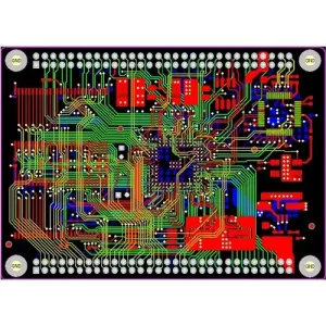
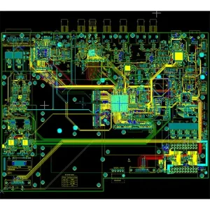
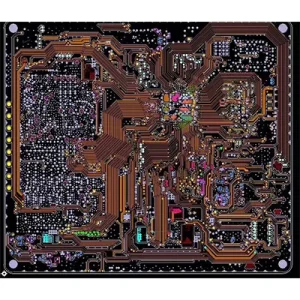
Optoelectronic multimedia FPGA processor, 10G SFP optical port
Photoelectric multimedia PCB board parameters:
PCB name: 6 layers
PCB Category: Through Hole Board
PCB board: Htg170
Board size: 146.3*167.4*1.6mm
Surface Treatment: Immersion Gold Process
PCB copper thickness: 1OZ
Minimum line width: 5MIL
Name: PCB design of digital set-top box
Digital set-top box PCB design features:
1. Only some small filter capacitors are placed on the reverse side, and the device is placed on the other side;
2, DDR3, HDMI, etc. do not punch holes, the same layer processing;
3. The integrity of the ground plane and the handling of the ground loop are strictly guaranteed.
Digital set-top box PCB board parameters:
PCB name: 2 layers
PCB Category: Through Hole Board
PCB sheet: FR4 1oz
Veneer size: 171*128*1.6mm
Name: 
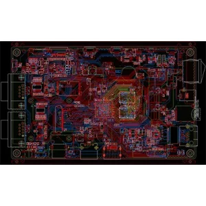
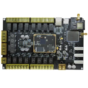
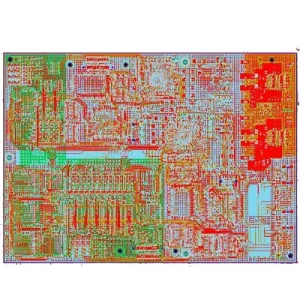
PCB design of industrial control motherboard
Industrial control motherboard PCB design features:
1. High integration and high density, the holes on the BGA plate and the filter capacitors are changed to irregular shapes;
2. 25G high-speed signal, 10-degree angle wiring, adopting the 10-degree angle design recommended by Intel is a conventional method to solve the glass fiber effect.
PCB board parameters:
PCB name: 14 layers
PCB Category: Through Hole Board
PCB board: Htg70
PCB thickness: 2.0MM
Name: 
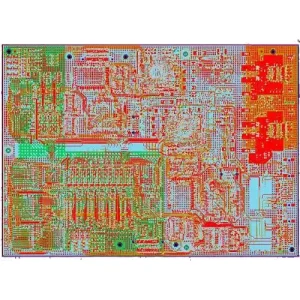
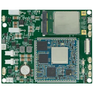
Multimedia motherboard PCB design
Features: 1. The highest signal rate is 5G (optical port signal); 2. The grounding of the optical port casing has been specially treated to ensure that EMI affects the product.
Number of PCB layers: 10 layers
PCB board: Htg170, 1oz
PCB surface: immersion gold process
PCB parameters: 4/4mil, Via: 8mil
Impedance control: +/-5%
Power: 24VDC
Device interface: RS485*3 (dimming color sensor)
Network interface: RJ45*1 (100M)
Name: 
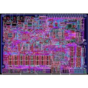
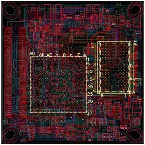
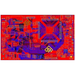
Six-layer core module PCB design
Requirements: Length matching of data, address, clock, and packet-level processing
Number of PCB layers: 6 layers
PCB surface: immersion gold process
PCB board: Htg170, 1.6mm, 1oz
PCB parameters: 5/5mil, Via: 8mil
Impedance control: +/-10%
Power: 24VDC
Device interface: RS485*3 (dimming color sensor)
Network interface: RJ45*1 (100M)
Wireless communication: 4G *1 (full Netcom MQTT protocol) LORA *1
Name: PCB Design of Intelligent Environment Controller
Power: 24VDC
Device interface: RS485*3 (dimming color sensor)
Network interface: RJ45*1 (100M)
Wireless communication: 4G *1 (full Netcom MQTT protocol) LORA *1
Output: DO *16 (220VAC@10A)
Amplifier: 60W audio amplifier
Storage: 512M DDR3 8G EMMC
System: Linux
Relay output: remote control, timing control
Color matching function: 485 control color matching
Name: PCB Design of Chemical Air Detector
Power supply: 7.4V3000mAh low temperature polymer lithium battery
Storage: RAM: 4G ROM: 64G
Device interface: TYPE-C (charging)
Wireless communication: whole network 2G\3G\4G + dual-band WIFI
Camera: 5 million autofocus camera
Screen: 5.7 inches 2160*1080 pixels
GPS: GPS+Beidou
On the communication protocol: TCP/IP
Printer: Embedded 58mm thermal printer
Card reading: embedded ID card information identification module
Name: Communication high-speed signal PCBA design
Plate: TG170 /TG180, F4BM, FR4, FR1-4, etc.
Designable layers: 1-32 layers
Minimum line width and line spacing: 3mil
Minimum laser aperture: 4mil
Minimum mechanical aperture: 8mil
Copper foil thickness: 18-175цm (standard: 18цm35цm70цm)
Peel strength: 1.25N/mm
Minimum punching hole diameter: single side: 0.9mm/35mil
Minimum hole diameter: 0.25mm/10mil
Aperture tolerance: ≤φ0.8mm±0.05mm
Name: Arbitrary Interconnect HDI PCBA Design
Plate: TG170 /TG180, F4BM, FR4, FR1-4, etc.
Designable layers: 1-32 layers
Minimum line width and line spacing: 3mil
Minimum laser aperture: 4mil
Minimum mechanical aperture: 8mil
Copper foil thickness: 18-175цm (standard: 18цm35цm70цm)
Peel strength: 1.25N/mm
Minimum punching hole diameter: single side: 0.9mm/35mil
Minimum hole diameter: 0.25mm/10mil
Aperture tolerance: ≤φ0.8mm±0.05mm
Name: 16-layer two-stage high-precision PCB design
Plate: TG170 /TG180, F4BM, FR4, FR1-4, etc.
Designable layers: 1-32 layers
Minimum line width and line spacing: 3mil
Minimum laser aperture: 4mil
Minimum mechanical aperture: 8mil
Copper foil thickness: 18-175цm (standard: 18цm35цm70цm)
Peel strength: 1.25N/mm
Minimum punching hole diameter: single side: 0.9mm/35mil
Minimum hole diameter: 0.25mm/10mil
Aperture tolerance: ≤φ0.8mm±0.05mm
Name: TG180 High Density Interconnector PCBA Design
Plate: TG170 /TG180, F4BM, FR4, FR1-4, etc.
Designable layers: 1-32 layers
Minimum line width and line spacing: 3mil
Minimum laser aperture: 4mil
Minimum mechanical aperture: 8mil
Copper foil thickness: 18-175цm (standard: 18цm35цm70цm)
Peel strength: 1.25N/mm
Minimum punching hole diameter: single side: 0.9mm/35mil
Minimum hole diameter: 0.25mm/10mil
Aperture tolerance: ≤φ0.8mm±0.05mm
Name: Automation Equipment HDI PCBA Design
Sheet: IT180, F4BM, FR4, FR1-4, etc.
Designable layers: 1-32 layers
Minimum line width and line spacing: 3mil
Minimum laser aperture: 4mil
Minimum mechanical aperture: 8mil
Copper foil thickness: 18-175цm (standard: 18цm35цm70цm)
Peel strength: 1.25N/mm
Minimum punching hole diameter: single side: 0.9mm/35mil
Minimum hole diameter: 0.25mm/10mil
Aperture tolerance: ≤φ0.8mm±0.05mm